When hardware engineer Gang first came into contact with multi-layer PCBs, it was easy to get dizzy. There are often ten or eight floors, and the lines are like spider webs. Draw several internal structure diagrams of multi-layer PCB circuit boards, and use three-dimensional graphics to display the internal structure of PCB diagrams with various stacked structures.
The core of the high-density interconnect (HDI) is in the via
The circuit processing of multi-layer PCB is no different from that of single-layer and double-layer. The biggest difference is in the process of via holes.
The lines are all etched, and the vias are all drilled and copper-plated. Everyone who does hardware development understands these, so I won’t go into details.
Multilayer circuit boards usually include through-hole boards, first-order boards, second-order boards, and second-order stacked hole boards. Higher-level boards such as third-order boards and any-layer interconnect boards are rarely used, and they are very expensive, so we won’t discuss them here.
In general, 8-bit MCU products use 2-layer through-hole boards; 32-bit MCU-level smart hardware uses 4-6-layer through-hole boards; Linux and Android-level smart hardware uses 6-layer through-holes to 8-layer through-hole boards. HDI boards; compact products such as smartphones generally use 8-layer-level to 10-layer 2-level circuit boards.
Most Common Through Hole
There is only one kind of via, from the first layer to the last layer. Regardless of whether it is an external circuit or an internal circuit, the holes are punched through, which is called a through-hole plate.
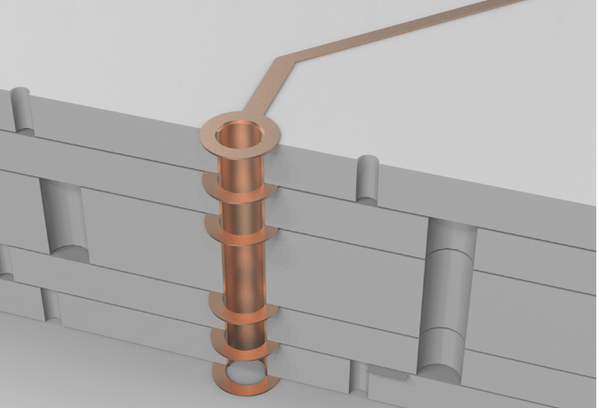
The number of through-hole boards has nothing to do with the number of layers. Usually, the 2-layer boards used by everyone are through-hole boards, while many switches and military circuit boards have 20 layers, which are still through-hole boards. Use a drill to drill through the board, then plate copper in the holes to create vias.
It should be noted here that the inner diameter of the through hole is usually 0.2mm, 0.25mm and 0.3mm, but generally 0.2mm is much more expensive than 0.3mm. Because the drill bit is too thin and easy to break, the drill is also slower. The time spent and the cost of the drill are reflected in the increase in the price of the circuit board.
Laser hole for high density board (HDI board)
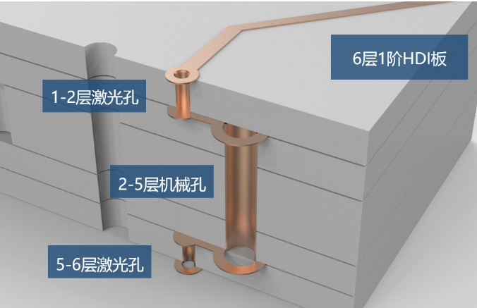
This picture is a stacked structure diagram of a 6-layer 1-stage HDI board. The two layers on the surface are laser holes with an inner diameter of 0.1mm. The inner layer is a mechanical hole, which is equivalent to a 4-layer through-hole board, and the outside is covered with 2 layers.
The laser can only penetrate the glass fiber plate, not the metal copper. Therefore, punching holes on the outer surface will not affect other internal circuits. After the hole is drilled by the laser, the copper is plated to form a laser via.
2-layer HDI board with two layers of laser holes
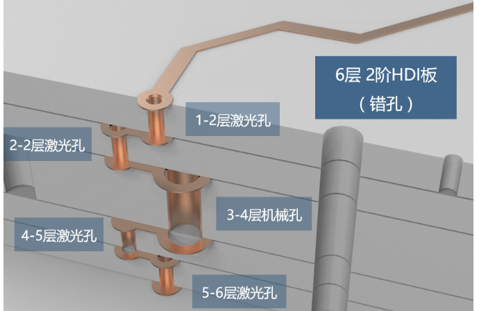
The picture above is a 6-layer 2-stage staggered-hole HDI board. Usually, people use 6 floors and 2 floors, and most of them start from 8 floors and 2 floors. There are more layers here, which is the same as 6 layers. The so-called 2nd order means that there are 2 layers of laser holes.
The so-called wrong hole means that the two layers of laser holes are staggered.
Why should it be staggered? Because the copper plating is not enough, the inside of the hole is empty, so you can't directly drill holes on it, you have to stagger a certain distance, and then make a layer of holes. 6 floors of the second stage = 4 floors plus 2 floors outside the first stage.
8 floors of the second stage = 6 floors plus 2 floors outside the first stage.
The process of stacked hole plate is complex and the price is higher
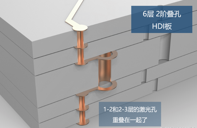
The two layers of laser holes of the staggered hole plate are overlapped together. Lines will be tighter.
It is necessary to electroplate and fill the inner laser hole, and then make the outer laser hole. The price is more expensive than the wrong hole.
Ultra-expensive multi-layer laser stacked holes for any layer interconnection board
That is, each layer is a laser hole, and each layer can be connected together. You can route the wires as you want, and punch holes as you want.
Layout engineers feel great just thinking about it! No longer afraid of not being able to draw!
Purchasing makes me cry when I think about it, it is more than 10 times more expensive than ordinary through-hole boards!
Therefore, only products like the iPhone are willing to use them. For other mobile phone brands, I have never heard of anyone who has used any layer of interconnection boards.
Summarize
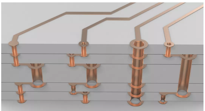
Finally, put a picture and compare it carefully—let’s go down.
Please pay attention to the size of the hole and whether the pad of the hole is closed or open.


