As an indispensable part of electronic products, PCB plays a key role in realizing the functions of electronic products, which leads to the increasing importance of PCB design, because the performance of PCB design directly determines the function and cost of electronic products. A good PCB design can keep electronic products away from many problems, thus ensuring that the product can be manufactured smoothly and can meet all the needs of the practical application.
Among all the elements that contribute to PCB design, Design for Manufacturing (DFM) is absolutely essential because it links PCB design with PCB manufacturing so that problems can be detected early and resolved in a timely manner throughout the life cycle of electronic products. As the manufacturability of electronic products is considered during the PCB design stage, the complexity of PCB design will increase. In the life cycle of electronic product design, DFM can not only make electronic products smoothly participate in automatic production and save labor costs in the manufacturing process, but also effectively shorten the manufacturing production time to ensure the timely completion of final electronic products.
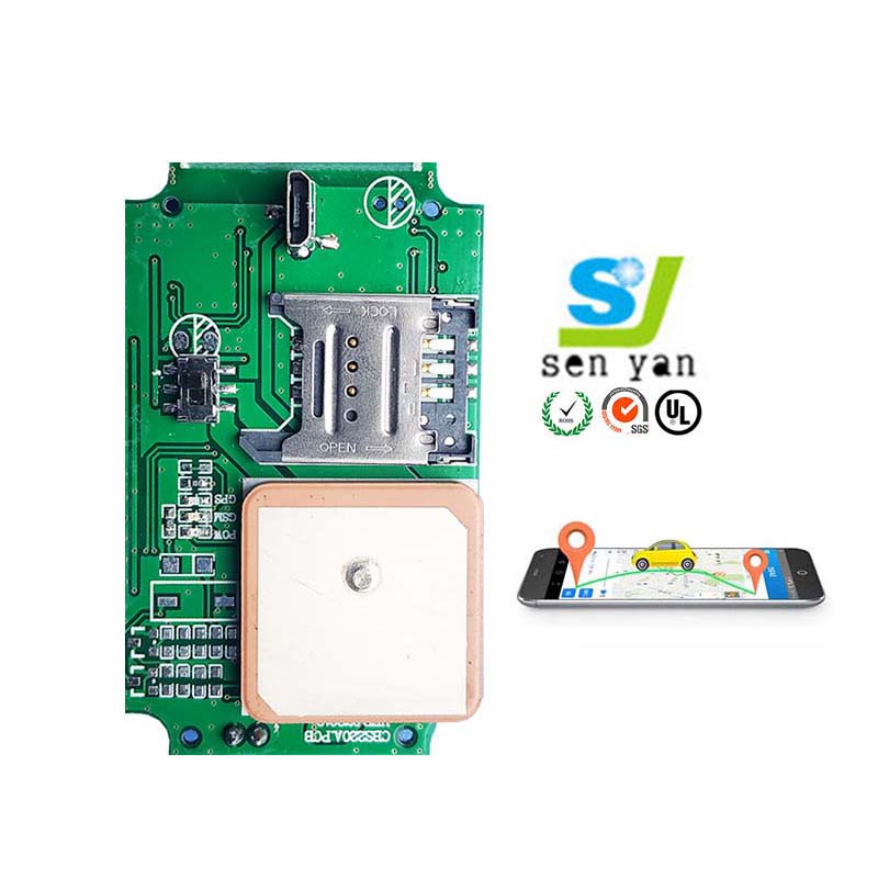
PCB Manufacturability
Since manufacturability is combined with PCB design, design for manufacturing is a key element leading to efficient manufacturing, high quality and low cost. The scope of PCB manufacturability studies is broad and can generally be divided into PCB fabrication and PCB assembly.
PCB manufacturing
As far as PCB manufacturing is concerned, the following aspects should be considered: PCB size, PCB shape, process edge and Mark point. Once these aspects are not fully considered during the PCB design stage, automatic chip mounters may not be able to accept prefabricated PCBs unless additional handling measures are taken. To make matters worse, some boards cannot participate in automatic manufacturing with manual soldering. As a result, the manufacturing period will be extended and labor costs will also increase.
1. PCB size
Each chip mounter has its own required PCB size, which varies according to the parameters of each mounter. For example, the maximum PCB size accepted by the chip mounter is 500mm*450mm, while the minimum PCB size is 30mm*30mm. That doesn't mean we can't handle PCB assemblies smaller than 30mm*30mm, and can rely on panelization when smaller sizes are required. When only relying on manual installation and the labor cost is rising and the production cycle is out of control, the chip mounter will never accept a PCB that is too large or too small.
Therefore, in the PCB design stage, the PCB size requirements set by automatic mounting manufacturing must be fully considered and must be controlled within an effective range.
The image above demonstrates the completed PCB panel design file. As a 5x2 puzzle, each square unit is a single board with a size of 50mm*20mm. The connection between each unit is realized by V-cut/V-scoring technology. In this image, the entire square shows that the final size of the panel is 100mm * 100mm. According to the above panel size requirements, it can be concluded that the panel size is within the acceptable range.
2. PCB shape
In addition to PCB size, all chip placement machines have requirements for PCB shape. A common PCB shape should be a rectangle with a length to width ratio of 4:3 or 5:4 (best). If the shape of the PCB is irregular, additional measures must be taken before SMT assembly, resulting in increased costs. In order to prevent this from happening, the PCB must be designed in a common shape during the PCB design stage in order to meet the SMT requirements. However, it is difficult to do this in practical situations. When the shape of some electronic products must be irregular, stamp holes must be used to make the shape of the final PCB have an ordinary shape. After assembly, redundant auxiliary baffles can be omitted from the PCB to meet automatic installation and space requirements.
The picture shows an irregularly shaped PCB, and processing edges are added through related software. The size of the whole circuit board is 8Omm * 52mm, and the square area is the size of the actual PCB. The size of the upper right corner area is 40mm * 20mm, which is the auxiliary process edge generated by the bridging of the stamp holes.
3. Process edge
In order to meet the needs of automatic manufacturing, process edges must be placed on the PCB to fix the PCB.
In the PCB design stage, a 5mm wide process edge should be reserved in advance, without any components and traces. Usually the technology rail is placed on the short side of the PCB, but the short side can be selected when the aspect ratio exceeds 80%. After assembly, the craft edge, which serves as an auxiliary production role, can be removed.
4. Reference point (Mark point)
For a PCB with components installed, Mark points should be added as a common reference point to ensure that each assembled device can accurately determine the position of components. Therefore, the Mark point is the SMT manufacturing benchmark required for automatic manufacturing.
Components need 2 Mark points, and PCB needs 3 Mark points, these marks should be placed on the edge of the PCB board and cover all SMT components. The center distance between the Mark point and the board edge should be at least 5mm. For PCBs with SMT components mounted on both sides, there should be Mark points on both sides. If components are placed too densely to place Mark points on the board, they can be placed on the process side.
PCB assembly
PCB assembly, referred to as PCBA, is actually the process of soldering components on a bare board. In order to meet the requirements of automated manufacturing, PCB assembly puts forward a new challenge for component packaging and component layout.
some requirements.
1. Component packaging
During the PCBA design process, if the component packaging does not meet the appropriate standards and the distance between components is too close, automatic mounting will not be performed.
In order to obtain the best component packaging, professional EDA design software should be used to be compatible with international component packaging standards. During the PCB design process, the bird's eye view area must not overlap with other areas, and the automatic IC placement machine will be able to accurately identify and perform surface mounting.
2. Component layout
Component layout is an important task in PCB design, because its performance is directly related to the complexity of PCB appearance and manufacturing process.
During the component layout process, the assembly surfaces of SMD components and THD components should be determined. Here, we set the front side of the PCB as component A side and the back side as component B side. Component layout should consider the assembly form, including single-layer single-package assembly,


